I found this article today.
Which, I considered is a break through!!
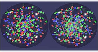
Nano Tech Kidney
Where dialysis falls short, nanotechnology promises to pick up the flag with a new approach to kidney disease treatment. Biophiltre, a California medical-device company, is developing a biomedical filter to mimic the function of the human kidney that would be less invasive.
NanoWireCancerDetectors
Harvard researchers used arrays of silicon nanowires to detect molecular markers of cancer with remarkable accuracy and speed. In minutes, a drop of blood could be scanned for an increasing number of known cancer markers through a novel electrical manipulation of the nanowires.
Read More....
NanoTech Application for Kidney & Cancer Detection!!
Tuesday, October 04, 2005
Wednesday, April 20, 2005

Picking apart the 'Big Bang' brings a big mystery
This research report is intersting.
However, I am in the opinion that the "experiments generated a "perfect" liquid of Linked Particles, Instead of a Hot Gas of Indepent particles!!" May be an oversight!!
According to the Sutra that I read both from the Gotama Buddha & Tao Guru Lao Tze. Their explanations is that is the combustions of gases that created the "Big Exposions" then after the expolsion the Billions of Universes are formed.
From colliding atoms: Instead of a hot gas of independent particles, top, experiments generated a 'perfect' liquid of linked particles.
Brookhaven National Laboratory.
Picking apart the 'Big Bang' brings a big mystery
By Dan Vergano, USA TODAY
An atom-smashing fireball experiment has physicists puzzling over existing theories about the moments after the "Big Bang" that scientists say created the universe. Researchers conducted the experiment over the past three years at the Energy Department's Brookhaven National Laboratory in Long Island, New York.
Thousands of collisions of gold atoms took place in the laboratory's Relativistic Heavy Ion Collider facility. The goal was to create a charged gas that was more than 1 trillion degrees, up to 150,000 times hotter than the sun's core. This was the climate scientists believe followed the Big Bang.
Instead, the collisions created pinprick-size fireballs with matter that behaved like a high-temperature liquid, rather than a gas, for its infinitesimally brief existence, the team reported Monday.
"It's a big puzzle and a big surprise," Brookhaven's Dmitri Kharzeev says. The results were reported at the American Physical Society meeting in Tampa and are scheduled for publication in the journal Nuclear Physics A.
Physicists hope that by understanding the sometimes unexpected behavior of fundamental particles at very high temperatures, they can unravel rules of matter that govern all conditions.
Their Big Bang experiment was a collaboration by four teams of scientists and pooled results from separate particle-detecting experiments. Hundreds of researchers were involved.
Their earlier findings suggested that the atomic collisions created a primordial concoction known as "quark-gluon" plasma. But rather than behaving like a charged gas, or plasma, and moving about on independent paths, subatomic particles inside the collisions moved collectively in response to pressure variations, like liquids.
"The fact that they can extract from those collisions glimpses of how this matter behaves is a major success by itself," says physicist Hans Georg Ritter of Lawrence Berkeley National Laboratory in California.
Quarks and gluons are the sub-particles inside protons and neutrons, which are the building blocks of atoms. Since the cool-down that followed the Big Bang 13.7 billion years ago, these subparticles are usually never seen liberated from protons and neutrons. They are bound inside these particles by strong atomic forces.
Trying to duplicate the moments that followed the Big Bang, the scientists used the high-powered collisions between heavy gold atoms to separate quarks and gluons from their proton and neutron containers. The scientists expected them to mingle as a continuous, charged gas, but that does not appear to have happened.
A few observers had expressed fears that the colliding atoms would create miniature versions of collapsed stars — tiny black holes that would consume Long Island, says Brookhaven's Sam Aronson. "But it's pretty clear that didn't happen."
Instead, the team is left with an intriguing discovery that they say will affect how physicists consider the first moments of the Big Bang. Kharzeev said physicists are still pondering how the early universe really developed if matter behaved as a liquid rather than a gas.
The post-collision particles acted like "perfect" liquids, which act almost uniformly in concert and dissipate heat very rapidly. Researchers are attempting to reconcile their findings with the behavior of the primordial fireball that lasted 380,000 years after the Big Bang.
In 2003, the WMAP satellite probe detected the signature of this fireball in the cosmic microwave background radiation that spans the entire sky.
Further, the discovery that the research team's collisions produced a perfect liquid rather than a gas is particularly intriguing, the researchers suggest, because it matches some aspects of string theory. This is an explanation of fundamental physics that treats physics particles as tiny strings instead of point-like objects and incorporates perfect liquids.
String theory aspires to become a "theory of everything" that unifies all forces of nature, says physicist Dam Thanh Son of the University of Washington, who was not on the discovery team. He said in an e-mail that the findings have not furthered this quest by string-theory proponents. But it could be that the results "will help us uncover a deep connection between the real world and string theory," he said. "That would be fantastic."
Despite the success of the experiments, cuts in Energy Department financing probably will reduce the program's operating time from 30 weeks to 12 weeks next year, Aronson says. "It will be a major hit on the productivity of the program, but we will continue."
USATODAY.com - Picking apart the 'Big Bang' brings a big mystery
Thursday, April 14, 2005
Speed of Light

NaNo Technology -- Digital Era!!
Everything On Electronics.
It would travel in Speed of Light!!
that Means That:
Less Authennuation,
Less Registance,
Less Heat Loss,
Less Current,
Less Power,
Less Energy,
Less Material,
Less resource,
Less Waste,
Less Pollutions.....
Towards Eternity.
Monday, April 11, 2005
Dark Matter...different from dark matters
These Is still matter.
It Is still Physical.
Nano Materials Are All Particles in Nano units of measurement.

It Is still Physical.
Nano Materials Are All Particles in Nano units of measurement.
Friday, April 08, 2005
Blogger Server Down
For the past 48 hours, Blogger server down.
Couple with the problem of Firefox Conflicts.. Therefore, I am unable to post.
Tomorrow, I will resume the posting.
Stay In tune. Thanks...
Couple with the problem of Firefox Conflicts.. Therefore, I am unable to post.
Tomorrow, I will resume the posting.
Stay In tune. Thanks...
Sunday, April 03, 2005
Disassemblers
In the mid 70's I was working on the Shoe Box computer with 16 Intel 8086 Processor Board. The assembler run on the PDP 11 Mini computer & the RT 11 Operating System, sometime take 1/2 a day to execute the code.
The article below is the Disassemblers for Nano-Computers.
These is something at the Nano-Electronics level.
Imagine, everything is at the Atom & Electron level.
My vision is that these is not the end. As soon as the Nano-Tech matured, Pico-Tech will emerge. As the applications of "Positron", "Negatron" are still in it infancy.

Disassemblers
Molecular computers will control molecular assemblers, providing the swift flow of instructions needed to direct the placement of vast numbers of atoms. Nanocomputers with molecular memory devices will also store data generated by a process that is the opposite of assembly.
Assemblers will help engineers synthesize things; their relatives, disassemblers, will help scientists and engineers analyze things. The case for assemblers rests on the ability of enzymes and chemical reactions to form bonds, and of machines to control the process. The case for disassemblers rests on the ability of enzymes and chemical reactions to break bonds, and of machines to control the process. Enzymes, acids, oxidizers, alkali metals, ions, and reactive groups of atoms called free radicals - all can break bonds and remove groups of atoms. Because nothing is absolutely immune to corrosion, it seems that molecular tools will be able to take anything apart, a few atoms at a time. What is more, a nanomachine could (at need or convenience) apply mechanical force as well, in effect prying groups of atoms free.
A nanomachine able to do this, while recording what it removes layer by layer, is a disassembler. Assemblers, disassemblers, and nanocomputers will work together. For example, a nanocomputer system will be able to direct the disassembly of an object, record its structure, and then direct the assembly of perfect copies, And this gives some hint of the power of nanotechnology.
The article below is the Disassemblers for Nano-Computers.
These is something at the Nano-Electronics level.
Imagine, everything is at the Atom & Electron level.
My vision is that these is not the end. As soon as the Nano-Tech matured, Pico-Tech will emerge. As the applications of "Positron", "Negatron" are still in it infancy.
Disassemblers
Molecular computers will control molecular assemblers, providing the swift flow of instructions needed to direct the placement of vast numbers of atoms. Nanocomputers with molecular memory devices will also store data generated by a process that is the opposite of assembly.
Assemblers will help engineers synthesize things; their relatives, disassemblers, will help scientists and engineers analyze things. The case for assemblers rests on the ability of enzymes and chemical reactions to form bonds, and of machines to control the process. The case for disassemblers rests on the ability of enzymes and chemical reactions to break bonds, and of machines to control the process. Enzymes, acids, oxidizers, alkali metals, ions, and reactive groups of atoms called free radicals - all can break bonds and remove groups of atoms. Because nothing is absolutely immune to corrosion, it seems that molecular tools will be able to take anything apart, a few atoms at a time. What is more, a nanomachine could (at need or convenience) apply mechanical force as well, in effect prying groups of atoms free.
A nanomachine able to do this, while recording what it removes layer by layer, is a disassembler. Assemblers, disassemblers, and nanocomputers will work together. For example, a nanocomputer system will be able to direct the disassembly of an object, record its structure, and then direct the assembly of perfect copies, And this gives some hint of the power of nanotechnology.
Wednesday, March 30, 2005
A Billion Bytes ... In A Box A Micron wide
I got my 1st Philips Audio Tape Recorder in 1961. & In 1961, I have my 1st Philips Transistor Radio. But both were destroyed by my gyougest brother.
I have witness the change of the Technology from
Electrical
Electronics Vacuum Tube
Electronics Transistor's
Transistor Logics
Integrated Circuits
Highly Integrated Circuits
Programmable Logic Arrays
Microprocessors
Multi-Microprocessors
And now the Nano-Technology....
I can see that perhaps after I am gone the Pico-Technology would be taking over the Nano-Tech era.
Now looking back those Electric-Mechanical base Data Storage Tapes.. then it was bigger then double the size of shoe box.
The Nano-Technology Mechanical Data Storage would at least billions times faster than the present electronic memory as well.
A Billion Bytes ... In A Box A Micron Wide* ... If two different side groups on a polyethylene-like polymer are used to represent the ones and zeros of binary code, then the polymer can serve as a data storage tape.
If one were to use, say, fluorine and hydrogen as the two side groups, and to allow considerable room for tape reading, writing, and handling mechanisms, then a half cubic micron would store about a billion bytes.
Access times can be kept in the microsecond range because the tapes can be made very short.
A mechanical random-access memory scheme allows storage of only about 10 million bytes in the same volume, though this can probably be bettered.
For a more detailed discussion, see "Molecular Machinery and Molecular Electronic Devices," by K. Eric Drexler, in Molecular Electronic Devices II, edited by Forrest L. Carter (New York: Marcel Dekker, 1986).
Engines of Creation - K. Eric Drexler : References
Saturday, March 26, 2005
Engines of Creation - Nano Computer
The following article is adapted from:

Foresight Institute.
I would agreed with the statement that 1/1,000,000 of the mechannical space. The NanoMechanical Computer would work faster than the electronic computer of today!!
I also foresees that the Electronics NanoComputers would work atleast 1,000,000 times faster then today Microprocessor based computer.
These Nano Computers would use perhaps less than1/100,000 of the power consumption of the current PC power. Thus reduce the usage of energy to operate them.
Nanocomputers
Assemblers will bring one breakthrough of obvious and basic importance: engineers will use them to shrink the size and cost of computer circuits and speed their operation by enormous factors.
With today's bulk technology, engineers make patterns on silicon chips by throwing atoms and photons at them, but the patterns remain flat and molecular-scale flaws are unavoidable. With assemblers, however, engineers will build circuits in three dimensions, and build to atomic precision. The exact limits of electronic technology today remain uncertain because the quantum behavior of electrons in complex networks of tiny structures presents complex problems, some of them resulting directly from the uncertainty principle. Whatever the limits are, though, they will be reached with the help of assemblers.
The fastest computers will use electronic effects, but the smallest may not. This may seem odd, yet the essence of computation has nothing to do with electronics. A digital computer is a collection of switches able to turn one another on and off. Its switches start in one pattern (perhaps representing 2 + 2), then switch one another into a new pattern (representing 4), and so on. Such patterns can represent almost anything. Engineers build computers from tiny electrical switches connected by wires simply because mechanical switches connected by rods or strings would be big, slow, unreliable, and expensive, today.
The idea of a purely mechanical computer is scarcely new. In England during the mid-1800s, Charles Babbage invented a mechanical computer built of brass gears; his co-worker Augusta Ada, the Countess of Lovelace, invented computer programming. Babbage's endless redesigning of the machine, problems with accurate manufacturing, and opposition from budget-watching critics (some doubting the usefulness of computers!), combined to prevent its completion.
In this tradition, Danny Hillis and Brian Silverman of the MIT Artificial Intelligence Laboratory built a special-purpose mechanical computer able to play tic-tac-toe. Yards on a side, full of rotating shafts and movable frames that represent the state of the board and the strategy of the game, it now stands in the Computer Museum in Boston. It looks much like a large ball-and-stick molecular model, for it is built of Tinkertoys.
Brass gears and Tinkertoys make for big, slow computers. With components a few atoms wide, though, a simple mechanical computer would fit within 1/100 of a cubic micron, many billions of times more compact than today's so-called microelectronics. Even with a billion bytes of storage, a nanomechanical computer could fit in a box a micron wide, about the size of a bacterium. And it would be fast. Although mechanical signals move about 100,000 times slower than the electrical signals in today's machines, they will need to travel only 1/1,000,000 as far, and thus will face less delay. So a mere mechanical computer will work faster than the electronic whirl-winds of today.
Electronic nanocomputers will likely be thousands of times faster than electronic microcomputers - perhaps hundreds of thousands of times faster, if a scheme proposed by Nobel Prize-winning physicist Richard Feynman works out. Increased speed through decreased size is an old story in electronics.
Engines of Creation - K. Eric Drexler : Chapter 1
Monday, March 21, 2005
Philips claims nano-technology memory breakthrough
In 1989 at the Nagoya, Technology for The Future. I have told the attendees that within 10 years, technology break through would make the present high power demand, 1st it would move from the 3V to 1V supply.
I also sees that by end of year 2000, the processor switching speed would reach Nano sec. & the chip would be in the sub-Micron level.
When I looking into the Bio-Chip level. I can foresee that the Switching Theory of Protein can be control using Bio-Signal.. then that is possible to make solid state Memory obsolute. But for the moment.. it is certain that Nano Tech Memory is going to be the key future.
The frontier is Bio-Memory. As no technologyt today can replace the Natural Memory cell of our boby. Perhaps the Stem Cell technology is the only means to be able to do the duplications process.
Philips Claims Nano-technology memory breakthrough
Smaller, faster, better - claim
By: Paul Hales Monday 21 March 2005, 07:53
BOFFINS AT PHILIPS RESEARCH say they are set to publish details of an "innovative" phase-change memory for future low voltage, low power deep sub-micron silicon chips.
The researchers from Eindhoven say that unlike current Flash memories, the performance of its proposed memory format "improves in virtually every respect, the smaller you make it".
The secret of Philips' memory cell, they say, lies in the structure and materials used. Previous memory cells based on phase-change materials have to apply a relatively high voltage to the phase-change material in its high-resistance amorphous state, in order to drive enough current through. For silicon chips produced in advanced CMOS process technologies these voltages are not practical, says Philips.
To overcome this problem, the company developed a doped Antimony/Tellurium phase-change material in which threshold switching between the amorphous and crystalline phases occurs at a low electric field strength of around 14V/μm.
Philips' new solid-state memory cell employs similar phase-change materials as current rewriteable DVDs, it says. The materials are deposited as an ultra-thin film on the surface of a silicon chip, and use an electric current to switch between phases and to detect the resultant change in its electrical resistance.
The company claims its new 'line-cell' phase-change memory has the potential to meet both the performance and scaling requirements of future nano-electronic silicon chips.
In a statement, Dr. Karen Attenborough, project leader of the Scalable Unified Memory project at Philips Research said: "The holy grail of the embedded memory industry is a so-called unified memory that replaces all other types, which combines the speed of SRAM with the memory density of DRAM and the non-volatility of Flash. Philips' new phase-change line-cell technology is a significant step towards this goal."
Philips will publish its research in the April edition of Nature Materials. µ
Philips claims nano-technology memory breakthrough
Tuesday, March 15, 2005
India Would Become leader In Nano-Tech In 5 Years
When I research into history, I found that both India & China shares a lots of common in Mathematics & Sciences; Technology development back to 5,000 to 6,000 years ago.
The reason that why these Sciences & Technogies are not advance is mainly due to the oppression of the Emperor Court system. As well as the life philosophies & emphasis on art.
With the recent years of open up, I am sure India would certainly make it to their success in Nano Technology.
India would become leader in nano-technology in 5 yrs
Monday, March 14, 2005 14:18:51 IST
Bio-chips developed through this technology could be used for retina correction, dental implants and also to activate the neurons in brain
S.P. Chaudhary, Executive Director-Retail, HPCL, exchanging agreements with Sania Mirza, while S. Roy Choudhury, Director-Marketing, HPCL and P.T. Suresh, DGM-Allied Retail Business look on.COIMBATORE (PTI): With bio-info-nano technologies expected to be the base for the future development, India is making efforts to come out with devices using nano-technology, including health and industrial applications, a senior scientist in the Defence Research and Development Organisation (DRDO) said last week.
India, for that matter, DRDO, which has realised carbon nano tube, has drawn up an action plan and making efforts to develop various applications, under the guidance of President, A. P.J. Abdul Kalam, DRDO chief controller (R and D) Dr.A. Sivathanu Pillai told reporters here.
Thirtytwo specialised institutions across the country were being involved in the research in the field, he said adding DRDO was working out on the investment requirement to enter into device making in a big way, by which India would become one of the leaders in the field within five years. Defence Research Development Establishment at Gwalior has developed a kit, by which one can identify typhoid within three minute, the fastest in the World, Pillai said, adding talks were on for its largescale commercial production.
Similarly, Defence Metallurgy Laborataries at Hyderabad has developed a stent (for dilation of arteries) at a cost of Rs.10,000, resulting in sudden reduction in the cost of the imported stent from Rs.1 lakh to Rs.30,000, Pillai said. The stent has already been used in 7,000 patients. It would be brought out in different types, with special coatings, he said.As a spinoff of missile technology, the organisation has developed calipers, weighing about 300 gms at a cost of Rs.250, Pillai said. This device was distributed among 6,000 children through nine nodal agencies across the country, with the help of Dr. Sethi, inventor of the Jaipur foot.Citing an incident of 12-year old Bheemappa of Belgaum in Karnataka, who had lost both his legs, Pillai said that using special calipers, he was able to walk and had received Kalam, who had specially visited the town to see him.
The lab in Hyderabad is presently engaged in stem cell research, which was in advanced stage, he said. Bio-chips developed through nano-technology could be used for retina correction, dental implants and also to activate the neurons in brain of those having mental problem. "We are heading towards a nano-bio revolution," he said adding through this technology a shoe can also be developed, by which one can walk with a speed of 40 km per hour.Pillai, also the managing director of Brahmos, the joint venture with Russia, said that the Air Force variant of the missile would be ready for testfiring within two years.
Cybernoon.com
Thursday, March 10, 2005
Tuesday, March 08, 2005
UCSD medical/bioengineering reseachers show titanium debris satobtage artificial joints
I can forsees that Nano Tech can not only improve our joints wear & tear, it would also help us to Live Longer & for our wellness & reverse the aging process, especially for the baby bloomer generation & beyond.
Look Young, Feel Young, Be Young in The Nano Tech era!!!!!
UCSD medical/bioengineering reseachers show titanium debris satobtage artificial joints
08 Mar 2005
Microscopic titanium particles weaken the bonding of hip, knee, and other joint replacements, according to research published online in Proceedings of the National Academy of Sciences by researchers at the University of California, San Diego (UCSD) School of Medicine and the Jacobs School of Engineering. The team demonstrated that titanium implants are safe in large blocks, but at the microscopic level, wear and tear can generate micrometer-sized particles.
"As replacement joints are becoming increasingly common in aging populations, our results explain how such devices fail and suggest that improvements should be made in artificial joint design," said the study's senior author K.L. Paul Sung, Ph.D., UCSD professor of orthopedic surgery and adjunct professor of cellular bioengineering.
The team measured how titanium particles affected the bonding strength of pins implanted in rat thighs. The pins were shown to come out more easily when the titanium particles were present, with the smallest and largest particles causing the greatest weakening. The researchers demonstrated how different-sized titanium particles affected bone-building cells called osteoblasts and bone-destroying cells called osteoclasts. Microscopic studies revealed osteoblasts did not form proper adhesions, with small- and medium-sized titanium particles concentrated inside cells. Increased production of the protein RANKL by osteoblasts recruited and activated osteoclasts at the insertion sites, further weakening the bone. Larger titanium particles also activated metalloproteinases, which chop up the extracellular matrix that holds cells together.
Currently, Sung is leading a team in using nano-technology to improve implant material which has three to five times higher wear resistance and fatigue properties to reduce particle generation from implants.
In addition to Sung, additional authors were first author Moon G. Choi, M.D., UCSD Department of Orthopedic Surgery; and Hae S. Koh, M.D., UCSD Department of Orthopedic Surgery; Daniel Kluess, M.S. and Daniel O'Connor, M.A., UCSD Department of Bioengineering; Anshu Mathur, Ph.D., George Truskey, Ph.D., Department of Biomedical Engineering, Duke University; Janet Rubin, M.D., Department of Medicine, Emory University School of Medicine and Veterans Administration Medical Center, Atlanta; and David X.F. Zhou, Ph.D., UCSD Department of Bioengineering.
The study was supported by a Bristol Meyers/Zimmer Award for Excellence in Orthopaedic Research and the National Institutes of Health.
Contact: Sue Pondrom
spondrom@ucsd.edu
619-543-6163
University of California - San Diego
http://www.ucsd.edu
UCSD medical/bioengineering reseachers show titanium debris satobtage artificial joints
Wednesday, March 02, 2005
Fujitsu Touts Carbon Nano Tubes For Chip Wiring - Form Factor Reduce By 1/3!!
This certainly a great breakthrough for the electronics industries.....
Copper wire not only have been high loses for transmitions of current in the chips or PCB, it also generate heat as well. In the past the PCB & chips form factors is limited by the lithography techniques for drawing the PCB real estate & the Chips Real Estate, with the Nono Tubes which is achieving the size of 1/3 of the size of Copper Tube.
Then, we can see that the the form factors of the VChips & PCB would reduce further by a 1/3.
Fujitsu touts carbon nanotubes for chip wiring
Paul Kallender, IDG News Service 02/03/2005 09:14:16
Fujitsu believes it has the answer to a major technology problem that will confront chip makers in the future -- using carbon nanotubes to replace copper wires in chip circuits.
For chips scheduled to be made around 2010, connecting wires made of copper will become so thin and their volume so small that the electrons will tend to migrate and leak out of the wires, said Yuji Awano, a research fellow at Fujitsu Laboratories' Nanotechnology Research Center, in an interview at the Japan Nano Tech 2005 exhibition held in Tokyo Feb. 23 to Feb. 25.
Because copper transmits electrons relatively inefficiently, the wires heat up and will become unusable as the electrons get pushed out of the tiny copper threads, according to Awano. Such problems will only worsen for the more advanced chips with even smaller circuits planned after 2010, he said.
Carbon nanotubes will become essential to replace copper in chips that are expected to be about a third of the size of those today, according to Awano.
Fujitsu, he said, is the first manufacturer to commit to using carbon nanotubes in place of copper wires in chips.
Carbon nanotubes are made when carbon atoms form hollow, open-ended cylinders. They have diameters between about 0.4 nanometers and 1.8 nanometers and can vary in length up to several hundred nanometers long, depending on how they are made. A nanometer is one-billionth of a meter.
"If you make a smaller chip, you need thinner wiring," Awano said. "We have to solve the electron migration issue, and to do this we need thicker wiring -- but we can't make thicker wiring because the chip size will become bigger."
Carbon nanotubes can carry about 1,000 times the current density, or the current per unit area, compared to copper, according to Awano. In addition, they transmit electrons about 10 times faster and dissipate heat much more readily -- characteristics that allow them to replace copper, he said.
Many of today's advanced chips are made on a 90-nanometer process. The measure refers to the average size of features on a chip built using that process.
Around 2010, chips will be made on a 45-nanometer process and around 2013, on a 32-nanometer process, according to the International Technology Roadmap for Semiconductors, a trade group that helps set standards for the chip industry.
Fujitsu will use the carbon nanotubes on some of its 45-nanometer process chips and most or all of its 32-nanometer chips, Awano said.
The manufacturer is already making carbon nanotubes to standard lengths that conduct electricity in the required way. It should be able to mass-produce them and develop the technology to put them in complex chips by the end of the decade, Awano said.
Fujitsu has already made test chips in which it has connected two layers of circuitry with about 1,000 connections using the carbon nanotubes as wires, he said.
"This is real, and it's a real challenge," said Makoto Okada, a manager at the company's public and investor relations division.
In addition to Fujitsu, several major technology companies, including NEC and IBM have announced breakthroughs in chip production processes and in their understanding of how carbon nanotubes work.
IBM, which pioneered the use of copper for connections in chips in the late 1990s, has yet to announce its plans, said Glen Brandow, a company spokesman.
Intel did not respond to questions on the subject.
NEC is also considering carbon nanotubes, but has not yet committed to the technology, said Toshio Baba, senior manager of NEC's Fundamental and Environmental Laboratories.
PC World
Tuesday, February 22, 2005
Tiny Is Beautiful: Translating 'Nano' Into Practical
In 1989 at Nagoya Technology for the Future Conference, I foresee the future of Technology go from Micro to Pico & Nao era in 20-30 years.
Now it is just the begining of the Nano Era.
I am confident that NaNo Technology is going to be the Key frontiers, be it in the Applications of:
Electronics,
Bio-Technology,
Instrumentations & Controls,
Robotics,
Energy,
Industrials,
Food,
Drinks,
Plants; Horticulture,
Nutritions & Supplements
Medicines,
Anti-Aging,
...etc.
The challenge is to use Physics to create NaNo objects near to the Atom or molecules size.
Scholars Probe Nanotechnology's Promise and Its Potential Problems
With a revolution in everything from toys to tumors on the horizon, scientists in the nanotechnology arena are working to gain the public's trust.
Hoping to both anticipate pitfalls and head off a publicity fiasco, policymakers and scientists are promoting research and public discussion on environmental, ethical, economic, and other societal implications of the burgeoning field of nanotechnology.
Students flock
Loosely defined as the purposeful creation of structures 100 nanometers in size or smaller, nanotechnology "is a real revolution because it is changing in a fundamental way how we build things," says Mihail Roco, who chairs the White House subcommittee that coordinates the multiagency National Nanotechnology Initiative (NNI). Scientists predict that applications of nanotechnology will go far beyond their current uses—in sunblock, stain−resistant clothing, and catalysts—to, for example, environmental remediation, power transmission, and disease diagnosis and treatment.
But realizing nanotechnology's potential requires public trust, says Vicki Colvin, director of Rice University's Center for Biological and Environmental Nanotechnology. The human genome project set a good example, she says, with 3−5% of its federal funds earmarked for studying implications of the research. That's in contrast to the nuclear energy and genetically modified organism industries, which are hobbled by bad public relations, she adds. "In GMO, they belittled the concerns of the people, and didn't take the risks seriously. I'd like nanotechnology to be a field that learns from the past."
To that end, some countries are beginning to invest in research into the broader impact of nanotechnology. This year, investment in nanotechnology by governments worldwide exceeds $3.5 billion, Roco says. NNI's fiscal year 2004 budget is $961 million, of which 11% goes to research on health and the environment; additional money is allocated to other studies relating to societal implications. Scholars in the humanities "were very encouraged by the language coming out of the NNI asking for there to be examination of implications early on," says Davis Baird, a philosophy professor and associate director of the University of South Carolina NanoCenter. "Roughly speaking, if you look at a new technology after it's gotten rolling, it's much more expensive to change things. At this stage, if you ask the right questions, you have more chance of nudging the technology in the right direction."
Magical materials
When matter is manipulated on the atomic scale, optical, electrical, magnetic, and other characteristics of materials change. "It's quantum mechanical in nature, and quantum mechanics is magic," says Stanley Williams, director of quantum science research at Hewlett−Packard Co in Palo Alto, California. "The new properties come out and make themselves available—and a lot of the time they are technologically useful. For example, if you take a hard material, a clay or a ceramic, and powder it down to the nanoscale, and mix it with a polymer, you wind up with a nanocomposite that can have a combination of hardness and toughness never seen in the natural world."
Other features that contribute to nanotechnology's promise are the expectation of cheap, low−polluting mass manufacturing and the possibility of making things, on the scale of biological building blocks, that could imitate or augment living systems. So far, most applications involve enhancements of preexisting materials, but new developments are in the works. A sampling includes lighter, more fuel−efficient cars, iron particles for immobilizing pollutants, and a liquid slurry that, when painted onto a surface, would collect solar energy.
Richard Smalley of Rice University, who won the Nobel Prize in Chemistry for his role in discovering fullerenes, talks about using conducting carbon nanotubes for efficient power transmission, and quantum dots and other nano−sized probes for testing and localizing disease. "We are imagining a time," he says, "maybe in just a decade or two, when the average person can go to a clinic and get a scan that tells the state of health in a noninvasive, low−cost way. This would have tremendous impact." In the more distant future, computers might be connected directly to the brain as a memory aid, he adds. "It would change what it means to be human."
Many questions, few answers
So what are the potential problems associated with nanotechnology? For now, questions far outnumber answers. What are the effects of nanostructures on human health and the environment? Are new protective measures needed to regulate nanotechnology? How do manmade nanomaterials differ from naturally occurring ones? How will individual privacy be protected from surveillance nanosensors? How will inexpensive mass manufacture of nanomaterials change the workforce? How will nanotechnology−related businesses affect local and global economies? Read More
The New York Times > Science > Tiny Is Beautiful: Translating 'Nano' Into Practical
Subscribe to:
Posts (Atom)
